The University of Nottingham
 Exchange online
Research Exchange
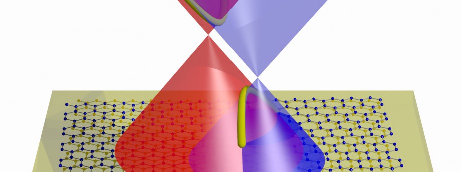
Layered graphene sandwich feeds hunger for designer materials
September 8 2014
Sandwiching layers of graphene with hexagonal boron nitride (hBN) could produce designer materials which can become the basis for novel high-frequency electronic devices.
The research, involving The University of Manchester, Lancaster University and The University of Nottingham, has been published in the prestigious academic journal Nature Nanotechnology. The work has demonstrated how combining the two-dimensional materials in a stack could create heterostructures capable of being used in next generation high-frequency electronic components.
Laurence Eaves, who holds Professorial appointments in the Schools of Physics and Astronomy at both Manchester and Nottingham, said: “This important research arises from a beautiful combination of the classical laws of energy and momentum conservation with the quantum phenomenon of particle tunnelling through a potential barrier. We are optimistic that further improvements to the device design will lead to applications in high-frequency electronics.”
Wonder material graphene is the world’s thinnest, strongest and most conductive material, and has the potential to revolutionise a huge number of diverse applications; from smartphones and ultrafast broadband to drug delivery and computer chips. It was first isolated at The University of Manchester in 2004.
Hexagonal boron nitride, otherwise known as white graphene, is one of a family of two-dimension materials discovered in the wake of the isolation of graphene at the University in 2004. Manchester researchers have previously demonstrated how combining 2D materials, in stacks called heterostructures, could lead to functional materials capable of being designed to meet industrial demands.
Now, for the first time, the team has demonstrated that the electronic properties of the heterostructures can be changed enormously by precisely controlling the orientation of the crystalline layers within the stacks.
The researchers, led by University of Manchester Nobel laureate Sir Kostya Novoselov, carefully aligned two graphene electrodes separated by hBN which allowed for both energy and momentum conservation for the tunnelling electrons, which drastically modifies the electronic characteristics of the devices.
The findings could pave the way for devices which can be operated at extremely high frequencies.
The research was carried out with scientists from Lancaster and Nottingham Universities in the UK, and colleagues in Russia and Japan.
Professor Novoselov noted: “It is the specifics of the electronic spectrum in graphene which made it possible the operation of our devices.”
Professor Vladimir Falko, from Lancaster University, added: “Our observation of tunnelling and negative differential conductance in devices made of multilayers of graphene and hexagonal boron nitride demonstrates potential that this system has for electronics applications.
“It is now up to material growers to find ways to produce such multilayer systems using growth techniques rather than mechanical transfer method used in this work.”
The paper, ‘Twist-controlled resonant tunnelling in graphene/boron nitride/graphene heterostructures, by A. Mishchenko, J. S. Tu, Y. Cao, R. V. Gorbachev, J. R.Wallbank, M. T. Greenaway, V. E. Morozov, S. V. Morozov, M. J. Zhu, S. L. Wong, F. Withers, C. R. Woods, Y-J. Kim, K. Watanabe, T. Taniguchi, E. E. Vdovin, O. Makarovsky, T. M. Fromhold, V. I. Fal’ko, A. K. Geim, L. Eaves and K. S. Novoselov’ has been published on Nature Nanotechnology’s website.
Tags: graphene, heterostructures, hexagonal boron nitride, Lancaster University, Laurence Eaves, Layered graphene, Nature Nanotechnology, Schools of Physics and Astronomy, Sir Kostya Novoselov, The University of Manchester, white graphene
Leave a Reply
Other
Top prize for quantum physicist
A University of Nottingham physicist has won a prestigious medal from the Institute of Physics for […]
Zero carbon HOUSE designed and built by students comes home
Design and construct a low cost, zero carbon, family starter home, transport it to Spain, build […]